China’s Chip Strategy: How Far Silicon Sovereignty Has Actually Come by 2026
Extractable Zero‑Click Block
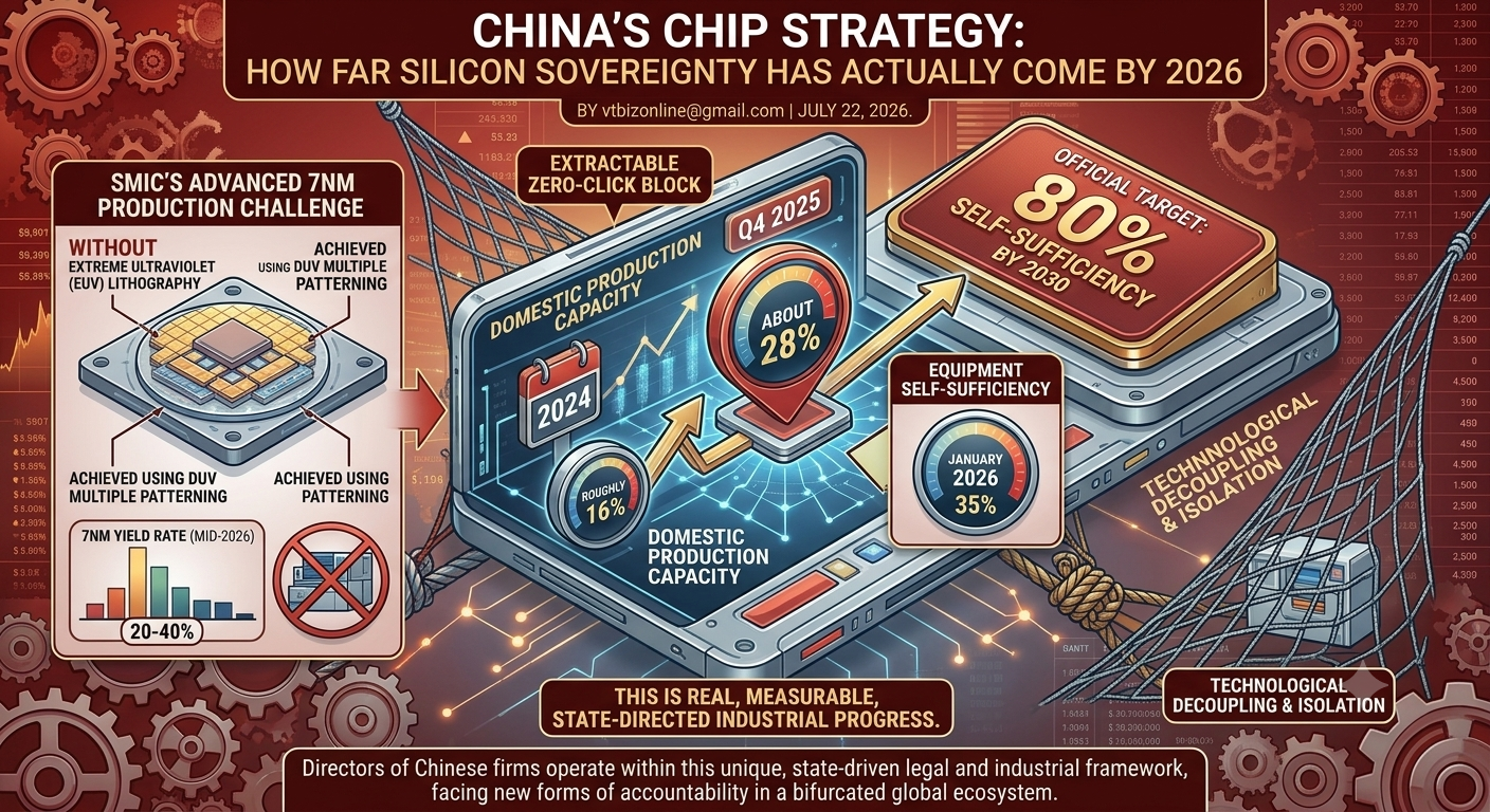
China’s semiconductor self‑sufficiency rate rose from roughly 16% in 2024 to about 28% in domestic production capacity by Q4 2025, with equipment self‑sufficiency separately reaching 35% by January 2026. The official target is 80% self‑sufficiency by 2030. This is real, measurable, state‑directed industrial progress; it is happening while SMIC’s advanced 7nm production still runs at yield rates of only 20‑40%, achieved without the extreme ultraviolet lithography tools export controls specifically deny China access to. Both things are true simultaneously: China’s chip strategy is working faster than most Western analysts expected in 2022, and it remains meaningfully behind the technological frontier it is racing to close.
I. What Does China’s Chip Strategy Actually Target?
Semiconductors sit underneath nearly every category of modern national capability: AI systems, defence electronics, telecommunications infrastructure, and advanced manufacturing. China’s leadership has treated this as a long‑horizon industrial priority since well before the current export‑control era, but the 2018‑onward escalation of US restrictions turned a strategic preference into an urgent necessity.
The core vulnerability US export controls exposed was straightforward: China’s access to the most advanced lithography tools, especially ASML’s extreme ultraviolet (EUV) systems, along with high‑end GPUs and certain fabrication technologies, could be constrained or cut off by policy decision in Washington and its allied capitals, largely independent of Chinese demand or capital. China’s response has been to attempt to build domestic capability across the entire semiconductor stack; not just chip design, but the equipment, materials, and fabrication processes beneath it, rather than relying on any single point of foreign dependency.
II. How Is SMIC’s Advanced‑Node Progress Actually Going?
SMIC, China’s flagship domestic foundry, is mass‑producing Huawei’s Ascend 910B AI chip on a 7nm‑class process and plans to double 7nm capacity in 2026, with total advanced‑node capacity estimated around 45,000 wafer starts per month in 2025, expanding toward 60,000 by the end of 2026.
The critical caveat is that SMIC achieves this 7nm‑class output using deep ultraviolet (DUV) tools and sophisticated multi‑patterning techniques; essentially, running older‑generation lithography equipment through the wafer multiple times to approximate what a single EUV pass would accomplish, because EUV tools remain off‑limits under export controls. This works, but it is slower, more expensive per chip, and yields have been reported in the 20‑40% range, well below the yields TSMC or Samsung achieve on comparable nodes with EUV access. SMIC has also entered pilot production on a 5nm‑class process, targeting partners including Huawei and Alibaba for 2026, using the same fundamentally constrained toolset.
Separately, Hua Hong has joined SMIC as a second domestic producer at the 7nm tier, and China has reportedly set a target to boost combined 7nm and 5nm output fivefold over two years.
III. What Does China’s Dual Strategy Actually Involve?
China is pursuing domestic capability and external acquisition simultaneously, and the mix is deliberate rather than improvised. On the domestic side, this means building fabs, subsidising equipment makers, and, as of 2026, mandating that new manufacturing capacity use at least 50% domestically produced equipment; a policy specifically designed to force Chinese toolmakers into the supply chain rather than leaving them permanently behind foreign incumbents.
On the acquisition side, China continues to pursue foreign expertise, equipment, and materials wherever export controls do not fully block the channel, alongside the well‑documented grey‑market flows of restricted chips into China through resellers and intermediaries that US enforcement actions have specifically targeted. This dual approach, building what can be built domestically while still acquiring what can still be acquired externally, reflects a realistic assessment that full self‑sufficiency by 2030 is a stretch target, not an assured outcome.
IV. Is China’s Talent Pipeline Actually a Structural Advantage?
This is one of the more solidly documented parts of the strategy. China graduates roughly 1.3 million engineers annually, compared to about 130,000 in the United States, and produces more than 77,000 STEM PhDs a year against roughly 40,000 in the US as of 2025.
This gap has been widening, not narrowing, for roughly two decades. It is a genuine structural advantage for any capital‑ and talent‑intensive industrial buildout, semiconductors included; but it is worth noting that raw graduate volume does not automatically translate into frontier semiconductor expertise, which depends on decades of accumulated institutional knowledge that US, Taiwanese, and South Korean firms currently hold disproportionately. Volume gives China a long‑term structural edge in absorbing and training talent at scale; it does not by itself close a technology gap measured in specific process‑node capability today.
V. What Are the Actual Consequences of Chip Export Controls?
Export controls have not stopped China’s semiconductor progress, but they have measurably shaped its direction and pace. Exclusion from EUV lithography and top‑tier fabrication tools forced Chinese firms into less efficient workarounds; the multi‑patterning DUV approach described above, which work but cost more and yield less than the frontier alternative. At the same time, that same exclusion has redirected enormous state investment into building domestic equipment and materials industries that likely would not have received comparable urgency or funding otherwise.
Whether this nets out as a win or a loss for the controls’ original goal (slowing China’s AI and military‑relevant chip capability) is genuinely disputed among analysts, and reasonable people read the same self‑sufficiency data differently. One reading treats the jump from 16% to 28% self‑sufficiency in roughly a year as evidence controls are accelerating exactly the domestic buildout they were meant to prevent. Another reading treats the persistence of a large sub‑80% gap, low 7nm yields, and continued dependence on smuggled hardware as evidence the controls are still meaningfully constraining China’s frontier capability, even if not eliminating its progress entirely.
VI. What Does This Mean for the Global Semiconductor Order?
The decades‑long dominance of a small number of Western and Taiwanese firms over the most advanced semiconductor nodes is not disappearing, but it is facing its first credible long‑term domestic challenger from China in this category. That does not mean parity is imminent; China’s 2026 output is still concentrated at 7nm‑class nodes with real yield and cost disadvantages, while TSMC and Samsung continue advancing at the frontier with better tools and higher yields. It does mean the assumption that advanced chip fabrication would remain a near‑monopoly of a handful of firms for the foreseeable future is no longer a safe one to build policy around.
The practical effect shows up first in AI hardware. Chips are the physical constraint on how much AI compute any country can field, and China’s ability to supply its own AI accelerators, even at a cost and yield disadvantage relative to Nvidia’s frontier products, changes the calculus of how effective export controls can be as a long‑term lever, since it gives Chinese AI developers a domestic fallback that did not reliably exist a few years ago.
VI‑B. Strategic Supply Chain & Hardware Risk for Enterprise Leaders
For global CTOs, hardware procurement heads, and enterprise risk officers, China’s semiconductor trajectory creates a distinct operational challenge: managing hardware fragmentation along geopolitical fault lines. As domestic production capacity hits 28% under a strict 50% local equipment mandate, multinational corporations operating within Asian markets face an increasingly bifurcated tech stack. Devices, IoT edge infrastructure, and enterprise servers built for the domestic Chinese market will increasingly rely on native 7nm and legacy nodes, while Western deployments remain anchored to TSMC, Samsung, and Western fab ecosystems.
This split introduces immediate vendor‑risk considerations. First, hardware multi‑homing is becoming mandatory; software architectures must now be optimised to run efficiently across asymmetric hardware performance profiles. AI models deployed globally must be engineered to account for the higher thermal envelopes and memory bandwidth constraints typical of non‑EUV silicon like Huawei’s Ascend series.
Second, legal and regulatory exposure is shifting from primary exporters to downstream enterprise consumers. As US BIS enforcement tightens around grey‑market hardware flows and secondary equipment sourcing, enterprises must conduct deeper supply‑chain audits to verify that hardware components do not trigger cross‑border sanctions or compliance violations.
Finally, enterprise leaders must plan for long‑term hardware cost inflation. The global transition away from a single, hyper‑efficient Taiwanese foundry model toward localised, heavily subsidised domestic fabs in both the East and West guarantees higher capital expenditure across the entire semiconductor value chain. Strategy in 2026 demands moving away from single‑source silicon reliance, building hardware‑agnostic software architectures, and treating chip supply chains as a primary vector of geopolitical enterprise risk.
VII. What’s the Honest Read on China’s Trajectory?
China’s chip strategy is neither the triumphant self‑sufficiency story its most enthusiastic domestic coverage suggests, nor the failed, controls‑strangled effort some Western commentary implies. It is a genuinely fast‑moving industrial buildout; self‑sufficiency roughly doubling in about a year by some measures, running up against real, persistent technical constraints: EUV exclusion, sub‑40% yields at the advanced node, and a 2030 target that most independent analysts consider ambitious but not implausible if current trajectories hold. The accurate framing treats this as a serious, well‑resourced, partially successful catch‑up effort under real constraint, not a settled outcome in either direction.
People Also Ask (PAA) Snippets
PAA 1: How does SMIC’s DUV multi‑patterning differ from TSMC’s EUV process?
DUV (Deep Ultraviolet) multi‑patterning exposes silicon wafers to older lithography tools multiple times to etch sub‑10nm features, whereas EUV (Extreme Ultraviolet) achieves this in a single, high‑precision pass. While SMIC successfully uses DUV multi‑patterning for 7nm production, it results in significantly lower yield rates (20‑40%), higher energy consumption, and elevated per‑chip manufacturing costs compared to TSMC’s EUV fabrication.
PAA 2: Can Chinese AI chips like the Huawei Ascend 910B replace Nvidia GPUs?
For core matrix math and local AI workloads, chips like Huawei’s Ascend 910B offer a viable domestic alternative. However, they face software‑level bottlenecks (such as competing with Nvidia’s mature CUDA ecosystem) and thermal efficiency challenges, meaning Chinese AI labs require larger physical clusters and more power to achieve comparable compute performance.
PAA 3: What is China’s 50% domestic equipment mandate for semiconductor fabs?
Enacted to force equipment self‑sufficiency, the policy requires new Chinese silicon foundries to source at least 50% of their machinery and tools from domestic vendors. This state directive guarantees market share for Chinese toolmakers, accelerating local R&D even if early‑generation equipment is less efficient than Western alternatives.
FAQ: China’s Semiconductor Strategy
Q1: What is China’s current chip self‑sufficiency rate?
Estimates vary by measure: roughly 28% in domestic production capacity as of Q4 2025 (up from about 16% in 2024), and about 35% in semiconductor equipment self‑sufficiency as of January 2026. The official target is 80% by 2030.
Q2: Can SMIC produce advanced chips without EUV lithography?
Yes, using deep ultraviolet (DUV) tools with multi‑patterning techniques, but at lower yields (reported at 20‑40% for 7nm‑class production) and higher cost than EUV‑based production from TSMC or Samsung.
Q3: What is SMIC currently producing at scale?
Huawei’s Ascend 910B AI chip on a 7nm‑class process, with capacity plans to double in 2026 and pilot 5nm‑class production underway for partners including Huawei and Alibaba.
Q4: How does China’s engineering talent pipeline compare to the US?
China graduates roughly 1.3 million engineers annually versus about 130,000 in the US, and produces more STEM PhDs annually (over 77,000 versus roughly 40,000 in the US as of 2025); a gap that has widened for about two decades.
Q5: Have US export controls stopped China’s chip progress?
No, but they have shaped its pace and method, forcing less efficient DUV‑based workarounds and redirecting massive state investment into domestic equipment and materials industries. Whether this counts as the controls working or backfiring is genuinely disputed among analysts.
Q6: Is China likely to reach 80% chip self‑sufficiency by 2030?
Uncertain. The trajectory from 2024 to 2026 shows meaningfully faster progress than many analysts expected, but reaching 80% would require sustaining that pace across increasingly difficult technical territory, including areas still dependent on tools China cannot yet replicate domestically.
CODA: Key Terms Defined
§1. DUV Multi‑Patterning
A technique using older deep ultraviolet lithography tools to etch sub‑10nm features by exposing the wafer multiple times. It is less efficient and more costly than single‑pass EUV lithography, with lower yield rates, but remains China’s primary workaround for advanced node production under export controls.
§2. Equipment Self‑Sufficiency Mandate
A Chinese policy requiring new semiconductor foundries to source at least 50% of their machinery and tools from domestic vendors. It is designed to force local toolmakers into the supply chain and accelerate domestic R&D.
§3. Hardware Fragmentation
The emerging divergence between tech stacks deployed in Western markets (reliant on TSMC/Samsung foundries and Nvidia GPUs) and those deployed in China (reliant on domestic 7nm and legacy nodes). This split creates vendor risk, cost inflation, and compliance challenges for multinational enterprises.